Resolving exciton diffusion in InGaAs quantum wells using micro-photoluminescence mapping with a lateral excitation
Shuo Cao, Xiaofan Ji, Kangsheng Qiu, Yunan Gao, Yanhui Zhao, Jing Tang, Zheng Xu, Kuijuan Jin*, and Xiulai Xu*.
We report a spatially-resolved photoluminescence mapping of InGaAs quantum wells. The photoluminescence was collected on top of the quantum well, with a HeNe laser pumping horizontally or vertically. In the horizontal configuration with a temperature at 68K, the spectral linewidth narrows from 2.8meV to 2.2meV with the peak shifting from 1.4425eV to 1.4415eV, while at 3.8K these changes were not observed. This demonstrates that photo-generated carriers can diffuse away from the laser spot and relax to the lower energy states in case that the charge carriers are thermally activated. The spectra narrowing in the vertical configuration that could not be observed is due to the fact that the emitted light was always collected from the same spot of the pumping laser without diffusion.

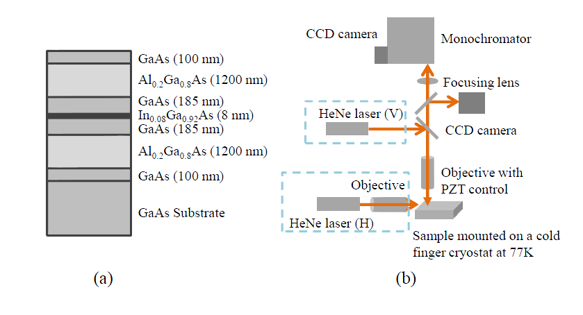
FIG. 1: (a) A schematic sketch of the InGaAs quantum well structure. (b) Optical setup for microphotoluminescence mapping with pumping laser exciting from the top (Vertical configuration) or from the side (Horizontal configuration) of the wafer. The microscopy objective were mounted on a xy piezoelectric stage to perform the PL (photon luminance) mapping.

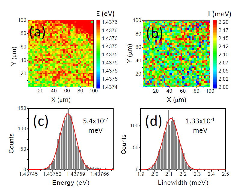
FIG. 2: (a) and (b) Emission energy and linewidth mapping in vertical configuration with an excitation power of 0.1 mW. The sample temperature was at 68K. The scanning area is about 100x100mm2 with a step of 2.5µm along each axis, 1681 points were collected in total. (c) and (d) The frequency histograms of the emission energy and the linewidth. The red lines are fitted results with Gaussian function. The values of full width at half maximum (FWHM) are insetting in the figures.


